


The Evolution and Importance of Chiplets in Modern Computing
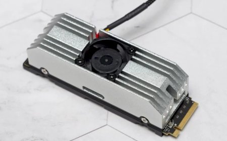
The computing world is witnessing a significant shift with the resurgence of chiplets, a technology that has been around for decades but used sparingly. Today, millions of people are utilizing chiplets in various devices, including desktop PCs, workstations, and servers. This technology is reshaping the industry, bringing forth a new era of innovation.
Understanding Chiplets: A Segmental Approach
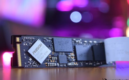
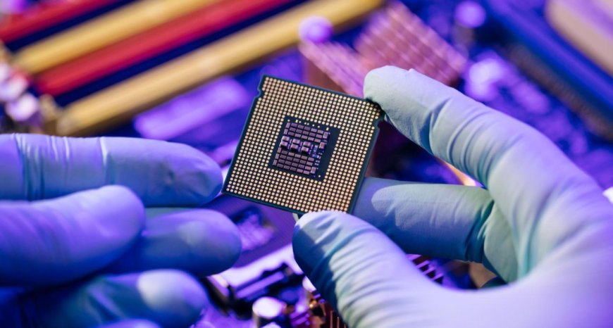
Chiplets represent a departure from traditional monolithic processor designs. In this segmented approach, specific processor parts are manufactured separately and then assembled into a single package using a sophisticated connection system. This method allows for the miniaturization of components that benefit from advanced fabrication techniques, enhancing efficiency and allowing for more complex designs. The remaining parts that do not require or cannot be miniaturized are produced using older, more cost-effective methods.
Advantages of Chiplets
The chiplet approach offers several benefits:
- Cost-Effectiveness: Despite the complex manufacturing process, the overall cost is typically lower than traditional methods.
- Flexibility: This approach provides a more manageable pathway for processor companies to expand their product range.
- Improved Performance: Segmented production allows for the integration of cutting-edge technology in specific areas, enhancing the overall performance of the processor.
Also Check Google's Gemini AI Model Launch Boosts Shares
Silicon Science: The Foundation of Chiplet Technology
To appreciate the shift towards chiplets, one must understand the basics of processor manufacturing:
- Silicon Wafers: CPUs and GPUs begin as large, ultra-pure silicon discs, approximately 12 inches in diameter.
- Layering Process: These wafers undergo a series of steps to add multiple layers of materials, creating intricate patterns through photolithography.
- Chip Binning: Each processor undergoes electrical testing to determine quality and categorize its performance.
- Die Cutting: The wafer is then sliced into individual dies, which are mounted onto substrates and undergo further packaging.
The Cost of Manufacturing
The manufacturing process is lengthy and expensive, with companies like TSMC and Samsung charging between $3,000 and $20,000 per wafer, depending on the process node used.
Process Nodes: The Evolution of Manufacturing
Process nodes have evolved over the years, with each new node offering benefits such as cost reduction, lower power consumption, or higher component density. However, not all processor parts scale down equally with advancements in process nodes.
The Challenge with Shrinking Components
While logic circuits continue to miniaturize, analog circuits and SRAM are reaching their limits, posing challenges in integrating all components into a single die.
The Rise of Memory in Processors
Recent processors have seen a significant increase in memory, such as SRAM. However, the disparity in scaling between logic and memory components makes it less cost-effective to produce everything on the same node.
Intel's Innovative Approach with the Pentium II
In 1995, Intel introduced the Pentium II, which featured a novel design incorporating a main chip and separate SRAM modules. This marked a shift towards using chiplets, allowing for the integration of components from different manufacturing nodes.
Conclusion: A New Era in Processor Design
The industry's move towards chiplets represents a divide-and-conquer strategy, enabling the integration of various components manufactured on different nodes. This approach mirrors Intel's Pentium II but on a much larger and more complex scale. As we continue to witness advancements in processor design, chiplets are poised to become the standard, heralding a new era of innovation in computing technology.