Nvidia Hopper and Lovelace back at TSMC?
Hopper and Lovelace, Nvidia's basis for graphics cards from the year 2022, are to be produced again at TSMC, in 5 nm.
Nvidia sought out Samsung as a partner for Ampere and had the graphics chips manufactured there in the 8 nm process. Even if much was never known about the partnership, the yield should not have been quite as good as one had hoped. And in principle, a smaller manufacturing process always has an advantage in terms of power consumption and thus also in terms of waste heat. So it comes as no surprise that Nvidia is said to have booked contingents for Hopper and Lovelace again at TSMC - in 5 nm.
At least that's what the Taiwanese industry service Digitimes reports, which usually gets its information from the island nation's well-networked semiconductor industry. Nvidia will probably go two ways in 2022 and offer Hoppers for data centers, while Lovelace will serve the gaming segment. The background to this should in turn be that the products can be tailored better to the target groups, hoppers potentially use the MCM process (multi-chip module) and Lovelace continues to be produced monolithically. https://twitter.com/chiakokhua/status/1465521242492993544?ref_src=twsrc%5Etfw%7Ctwcamp%5Etweetembed%7Ctwterm%5E1465521245156298754%7Ctwgr%5E%7Ctwcon%5Es2_&ref_url=https%3A%2F%2Fwww.pcgameshardware.de%2FNvidia-Geforce-Grafikkarte-255598%2FNews%2FHopoper-und-Lovelace-wieder-bei-STMC-in-5-nm-1384611%2F Lovelace
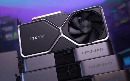
At least for the AD102, which was supposed to fuel the RTX-4000 flagship, there were already some rumors. A boost clock of up to 2.5 GHz for the design was circulating on the Internet. The high clock rates and the large chips urgently require modern manufacturing processes, because otherwise, the power consumption will soon be beyond 500 watts. The Geforce RTX 3090 already has a TDP of 350 watts; the RTX 3090 Ti is said to be 450 watts. That always leaves a bit of OC leeway and the GDDRX6 is not a food lover either, but in 8 nm Nvidia should quickly reach the limit of what is accepted by the market. The other day 550 watts made the rounds - it remains unclear whether this is true.
The AD102 is said to have 18,432 shaders in the rumor mill, packed in 144 clusters. It is not entirely clear whether we have the full configuration here, but to compare the GA102 as it is used in the RTX 3090 (not in full configuration): 10,496 shaders in 82 clusters at almost 1.4 GHz.
Particularly fast ampere chips produce around 1.5 GHz in the reference ex-works. It is very interesting that it should stay with the 384-bit wide memory interface. So probably not much will change from the status quo, except maybe faster GDDR6X chips with a higher density. Hopper
For Hoppers, "CoWoS" is specifically mentioned - CoWoS-S Rapid Progress is a process that TSMC offers to enable multi-chip designs - even with solutions with a computing chip, this is exciting if you have the HBM memory on the package you want to accommodate. AMD also uses the technology for 3D stacking, among other things. The recently introduced AMD Instinct MI250 (X) showed what this can look like in the end. The Twitter source mentions in another post that the packaging of both products should take place at ASE.
